


 English
 中文
中文marketing@dgkaihang.com
Enterprise Dynamics


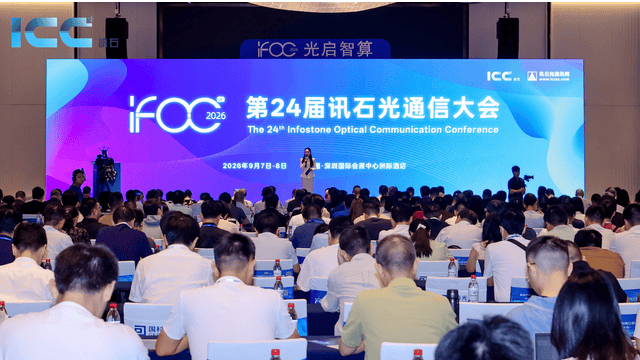
In September 2026, the 24th ICC Optical Communications Conference (IFOC 2026) and the 27th China International Optoelectronic Exposition (CIOE 2026) were held successively in Shenzhen.
The core proposition of the optical communications industry used to be "pushing speeds higher." With the rapid expansion of AI computing infrastructure, optical communications has officially entered a new stage of development — the Optical Communications 3.0 Era.
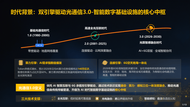
"Optical Communications 1.0 addressed 'whether we can connect.' 2.0 addressed 'whether we can connect fast.' 3.0 focuses on 'whether we can connect powerfully and intelligently.'" This was the systematic definition of "Optical Communications 3.0" given by Wu Jun, Chief Expert of ICC, at the IFOC 2026 main forum.
The changes of this era are not limited to the continued iteration of transmission speeds from 800G to 1.6T and beyond. More critically, optical interconnect is evolving from a traditional communication component into a deeply integrated element of switching chips, servers, racks, and complete data center architectures — becoming a core hardware component of AI computing infrastructure.
The evaluation criteria for industry competition have shifted accordingly: from single-component performance to overall system performance; from technical feasibility to engineering replicability; from laboratory sample validation to large-scale volume delivery. The IFOC and CIOE exhibitions collectively released this industry signal.
From the demand side, industry growth momentum is strong. Goldman Sachs released a report during the exhibition, significantly raising its global optical module market size forecast, projecting market sizes of approximately USD 67.7 billion, USD 131.4 billion, and USD 148.5 billion for 2026–2028 respectively — upward revisions of 33%, 81%, and 115% compared to previous forecasts.
Compared to the demand surge, supply-side contradictions deserve more attention. As AI cluster scale continues to expand, the optical interconnect industry's challenge is no longer limited to developing high-performance products, but rather how to reliably replicate mature technology solutions across hundreds of thousands to millions of units, ensuring long-term reliable operation in real data center scenarios.
TrendForce points out that optical engine yield and advanced packaging capacity have become the primary bottlenecks for CPO scale-up. Yole Group also notes that the difficulty in the AI era is not completing prototype development for optical components and optical engines, but achieving sustained reliability certification for high-yield optoelectronic components under large-volume conditions.
The core contradiction in the optical communications industry has completed its transition: from a game of technology route selection, upgraded to a competition of stable, large-scale delivery capability under chosen routes. This is the most fundamental industry proposition of the Optical Communications 3.0 Era.
I. From 1.0 to 3.0: Optical Communications Evolves from Component to Critical Computing Infrastructure
A clear developmental trajectory can be delineated for the optical communications industry.
Optical Communications 1.0 centered on connectivity. It replaced traditional electrical signals with optical fibers, solving long-distance, high-capacity information transmission and enabling remote information delivery.
Optical Communications 2.0 centered on speed. With the flourishing of the internet, cloud computing, and data centers, 100G, 400G, 800G, and 1.6T iterated and evolved. Industry competition revolved around optical chips, modulation devices, DSP, and optical modules, focusing on improving single-link data throughput.
Entering the AI computing era, the industry logic has transformed once again. GPU clusters have evolved from single racks to ultra-large-scale deployment. AI training and inference place stringent demands on inter-node interconnect. Traditional electrical interconnect is gradually hitting physical ceilings in transmission distance, power consumption, and bandwidth density. Optical interconnect is no longer merely a connecting component between devices — it has become critical hardware supporting computing system operation, namely Optical Communications 3.0.
The goal of the 3.0 era is not merely pursuing transmission speed, but enabling optical interconnect to embed into computing systems with lower power consumption, higher integration density, and higher reliability, achieving large-scale commercial deployment.
Accordingly, the boundaries of industry competition have been broadened. Chips are the foundational link, optical modules are the terminal product, and optical engines are important network nodes. The true industry competition is the entire set of industrial foundational capabilities spanning chips, packaging, connectivity, testing, thermal management, and system integration.
The six mainstream technology routes exhibited at IFOC and CIOE this year are not simply substitutive relationships, but rather represent the search for optimal implementation paths under different application stages and engineering constraints.
II. Six Technology Routes in Parallel: Competition Shifts from Route Selection to Engineering Fulfillment
As per-channel speeds upgrade toward 200G, traditional pluggable, LPO, NPO, XPO, CPO, and Optical I/O have formed a layered, coexisting industry landscape. China Merchants Bank International Research predicts that CPO, NPO, and pluggable solutions will coexist along multiple paths for the next 3–5 years. The industry focus should not be on which route ultimately wins, but on which solution can first cross the engineering threshold from sample to large-scale delivery.
1. Pluggable: Market Mainstay, Power Consumption Hits Engineering Boundary
Zhongji Innolight's Zhihe Photonics exhibited a full series of 1.6T/800G optical modules; Cambridge Technology released 1.6T-class OSFP optical modules; Eoptolink showcased samples up to 12.8T XPO.
Pluggable solutions remain the most mature technology route in data centers today, with the most complete supply chain support. However, after 1.6T module power consumption exceeds 30W, traditional air cooling and front-panel port density are gradually approaching engineering limits.
The competitive focus of this route has shifted from pure speed upgrades to low-power optimization, optical engine integration design, and efficient thermal solution development. Pluggable solutions still carry the largest real-world market demand; the next stage challenge is ensuring stable deployment and operation under high-power constraints.
2. LPO: Achieves Power Optimization, Shifts Challenge to System Coordination
LPO reduces system power consumption and latency by shortening electrical signal paths and eliminating some DSP functions. Compared to architecture-reconstruction solutions, LPO requires smaller changes to the existing pluggable supply chain, offering transitional advantages.
However, LPO is not simply "removing DSP." Actual performance depends heavily on coordinated adaptation among switching chips, host SerDes, driver chips/TIA, and optical modules, imposing stringent requirements on signal integrity across the entire electrical link. While component-level power decreases, system-level coordination difficulty rises significantly. This is a typical characteristic of the 3.0 era: single-component performance alone can hardly determine overall system performance.
3. NPO: Engineering Feasibility Constitutes Core Competitive Advantage
Compared to CPO, NPO's outstanding advantage is not limited to performance but extends to high compatibility with existing manufacturing and O&M systems. SemiAnalysis summarizes NPO's advantages: field replaceability, controllable fault scope, and lower assembly manufacturing difficulty. NPO can fully leverage mature HDI laminate boards and SMT production lines, with controllable line modification and process migration costs — making it the optical engine direction with the highest industrialization activity at this exhibition.
Accelink introduced a 6.4T silicon photonic single-mode NPO optical engine, employing 32×200G parallel channels and 2.5D Flip-Chip packaging processes, specifically addressing mass-production engineering challenges such as multi-channel signal integrity, high-density thermal management, and high-precision optical alignment. Huagong Genuine released a 6.4T NPO near-package optical engine, employing a DSP-free silicon photonic architecture with 32-channel 212.5G PAM4 electrical interfaces.
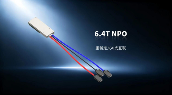
The value of these exhibits lies not merely in improved parameter metrics, but in focusing on engineering pain points constraining mass-production deployment. NPO's essential advantage is industrialization delivery certainty.
4. XPO: High-Density Pluggable Transitional Form
Huagong Genuine exhibited a 12.8T XPO solution, with bandwidth density 4 times higher than traditional 1.6T products, integrating liquid cooling thermal structures. XPO retains the O&M convenience of pluggable solutions, breaking through traditional module power limits through high-density integration and liquid cooling design. For data centers seeking to increase port density without adopting deeply integrated architectures, XPO provides a realistic upgrade path.
However, XPO overall remains in the early stages of standard completion and ecosystem cultivation. The XPO MSA organization was established in March 2026, with the first technical specification still circulating among founding members. Supporting 204.8T switch systems have not yet been deployed at scale, and upstream-downstream industry coordination has not yet aligned. Industry resources are prioritizing NPO and CPO, which have stronger engineering feasibility and clearer delivery timelines.
XPO's positioning is pragmatic — extending the lifecycle of traditional pluggable optical modules as a transitional choice before large-scale CPO adoption. As standards are finalized and switch systems based on Tomahawk 6 and Tomahawk 7 chips are gradually deployed, XPO's industry attention is expected to continue rising.
5. CPO: Dynamic Demonstration Completed, Mass Production is the Real Test
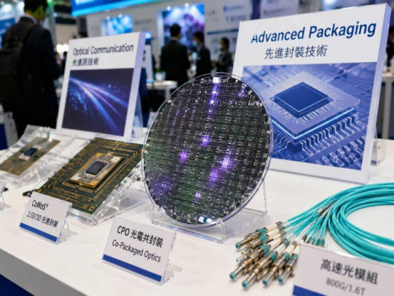
At the exhibition, Huagong Genuine completed a 3.2T CPO optical engine business dynamic demonstration. The product employs TGV glass substrate 2.5D advanced packaging, configured with ELSFP external light sources, with overall power consumption controlled within 5.5W.
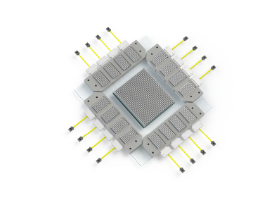
The evolution from static samples to real business flow demonstrations represents CPO's progression from technical feasibility to engineering validation. However, a significant gap remains before large-scale commercialization. CPO must simultaneously overcome multiple challenges beyond optical engine illumination: packaging yield, optoelectronic coupling, thermal management, cost control, laser reliability, and system O&M — all must match data center long-term operational standards.
CPO's next-stage evaluation dimension will shift from single technical metrics to comprehensive delivery capability: sustained supply with stable yield, controllable cost, and maintainable form factor. Compared to CPO, NPO better fits current data center engineering requirements. LightCounting forecasts that by 2030, NPO/CPO combined will occupy over 25% of the data center communications market, with 2026–2028 industry growth primarily driven by NPO.
6. Optical I/O: Toward Computing Chip Interconnect, Commercialization Still Requires Time
Optical I/O (OIO) represents the technology form in which optical engines are closest to computing chips along the optical interconnect evolution path, extending the optical interconnect boundary from switches down to GPU and XPU computing chips. Unlike pluggable/LPO/NPO/CPO, which primarily address switch ASIC and optical module interconnect, OIO aims to achieve direct optical communication between computing chips, breaking through electrical interconnect bandwidth and power bottlenecks.
At CIOE, Lanqun Micro exhibited the Denali optoelectronic fusion micro-ring OIO chiplet compliant with OCI MSA standards, employing micro-ring wavelength division multiplexing and monolithic optoelectronic integration to embed optical transceiver units into computing chip packaging systems. In March 2026, NVIDIA, Broadcom, AMD, Meta, Microsoft, OpenAI, and other companies jointly established OCI MSA to advance optical interconnect specifications for large-scale AI expansion, marking the emergence of the OIO industry ecosystem.
However, OIO industrialization is in its early stages, with unresolved challenges in micro-ring modulator wavelength stability, optoelectronic integration yield, interface standardization, interposer thermal management, packaging reliability, and upstream-downstream ecosystem coordination. Industry research reports predict commercial deployment at the earliest around 2030–2031. CPO achieves optoelectronic co-packaging within switches, while OIO further penetrates optical interconnect to the computing chip level. The transition from chip prototype to scale delivery depends on coordinated maturity of components, packaging, thermal management, and system standards.
| Architecture | Interconnect Object | Optical Engine Position | Core Positioning |
|---|---|---|---|
| LPO / XPO | Switch ↔ Optical Module | Front Panel Pluggable | Network Connectivity on Switch Side |
| NPO / CPO | Switch ASIC ↔ Optical Engine | On PCB / Same Substrate | Optoelectronic Integration on Switch Side |
| OIO | Computing Chip (GPU/XPU) ↔ Computing Chip | Inside Computing Chip Package | Direct Optical Interconnect Between Chips |
III. Optical Chips: 200G EML Demand Grows Rapidly, Mass Production Yield is the Core Threshold
Technology routes answer "how to achieve interconnect." Optical chips determine "whether stable manufacturing can be sustained." 200G EML is a typical microcosm of the current industry contradiction.
Current global 200G EML market demand is approximately 150 million units, but deliverable effective capacity is only 50–80 million units, with a supply-demand gap of 60%–70%. Product lead times have extended from 16 weeks to 40 weeks, and leading companies' orders are already booked through the end of 2027. Three US and Japanese manufacturers occupy over 80% of global high-end capacity. The domestic substitution window has opened, but the extent of substitution space ultimately depends on mass production yield.
Source Photonics is the first domestic enterprise to achieve large-scale mass production of 200G EML, disclosing at the exhibition a stable mass production yield of 85%–90%. Its 2026 output is expected to reach 18–22 million units, accounting for approximately 70% of global total capacity, with orders locked through 2028. Changguang Huaxin plans to achieve 200G EML mass production in Q4 2026. Yuanjie Technology targets mass production by the end of 2026. San'an Optoelectronics has completed reliability testing and initiated customer sampling. The supply landscape has expanded from Source Photonics' single-point lead to a four-tier echelon. The 6–9 month mass production progress gap between Source Photonics and Changguang Huaxin does not stem from technological generation gaps, but from production line accumulation and mass production validation systems.
Sample releases rely on performance metrics; product delivery relies on yield. From prototype samples to large-scale delivery lies a realistic chasm of yield consistency, capacity ramp-up, and complete customer reliability certification.
IV. InP, TGV, and Glass Bridge: Supply Chain Restructures Around High-Density Mass Production
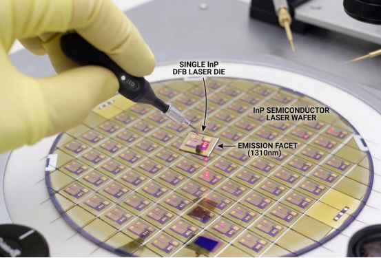
The large-scale expansion of 200G EML continues to transmit pressure upstream. Indium Phosphide (InP) is the core substrate material for high-speed EML and lasers, and supply capability has become a hard constraint on high-speed optical interconnect expansion.
Global high-end InP substrate capacity is highly concentrated, with lengthy new capacity construction and yield ramp-up cycles. With expanding demand for high-speed EML and silicon photonic external light sources, InP supply certainty has drawn full-industry-chain attention. Domestic enterprises are accelerating expansion, with Yunnan Germanium's subsidiary Xinyao Semiconductor continuously advancing InP wafer capacity construction.
Silicon photonic solutions can integrate modulators, waveguides, and detectors on silicon-based chips, reducing discrete component count and leveraging CMOS manufacturing processes to improve integration density — an important path for NPO and CPO high-density architectures. However, silicon material itself cannot emit light, and mainstream silicon photonic solutions still rely on InP-based continuous-wave lasers for light sources. Silicon photonics can reduce InP consumption per unit product but cannot completely eliminate InP materials.
InP epitaxial manufacturing relies on MOCVD equipment, with concentrated equipment supply and long delivery cycles, further constraining upstream capacity release, forming a complete industry chain transmission chain: High-speed EML demand surge → InP substrate demand rise → Epitaxial line expansion → MOCVD equipment procurement and delivery → New capacity deployment and release.
Optical interconnect delivery certainty is no longer just a challenge for downstream module manufacturers, but a full-industry-chain proposition spanning chips, materials, and equipment.
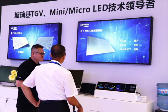
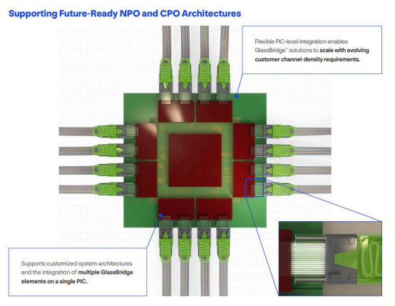
At the packaging level, TGV glass substrates and glass bridge technology have become important supports for high-density optical interconnect. Traditional organic substrates are gradually showing shortcomings in high-frequency, high-density, and high-reliability scenarios, while glass substrates offer dimensional stability and high-density interconnect advantages. Woge Optoelectronics has established a TGV panel-level production line with monthly capacity of 10,000 panels, minimum aperture of 5μm, and aspect ratio greater than 20:1, advancing NPO product mass production. Corning introduced a glass bridge solution that fabricates micro-optical waveguides inside glass to achieve high-density coupling between optical fibers and PIC chips, shortening optical path transmission distance.
From InP semiconductor materials and silicon photonic chips to TGV glass substrates and glass optical waveguides, the supply chain collectively responds to the same proposition: as optical interconnect moves toward chip-level high density, how do traditional materials, components, and packaging processes match large-scale manufacturing requirements. This is also a manifestation of the Optical Communications 3.0 Era, where competition upgrades from single-point performance comparison to material-process-equipment-mass production system coordination capability comparison.
V. Connectors: Upgrading from Mechanical Interface to Critical High-Density Optical Interconnect Component
In the Optical Communications 3.0 Era, the connector industry evolves alongside optical interconnect architecture iteration. As optical chip and optical engine integration density continues to increase, optical connectors are iterating toward miniaturization, high density, high precision, and high reliability, adapting to deeply integrated interconnect systems.
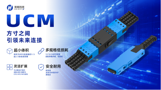
Multiple manufacturers launched new-generation interconnect products at the exhibition: Laitasi Optics released a 64-channel expanded beam optical fiber connector, introducing semiconductor manufacturing processes into connector production to enhance multi-channel docking capability. SENKO SN-MT achieves single-row 16-fiber optical connection within standard SN dimensions, improving spatial port density through interface miniaturization. Kaihang Technology's UCM micro multi-fiber connector achieves port density 3 times that of traditional solutions, supporting up to 4,224 fibers per 1RU with 16F, with typical single-mode insertion loss ≤0.25dB.
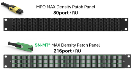
Against the backdrop of continued NPO, CPO, and OIO advancement, connectors, FAUs, and fiber cabling management need to match higher integration density and more complex system deployment conditions. Connector form factor, channel density, docking precision, and long-term reliability have already directly impacted high-density optical interconnect system integration and field deployment results.
VI. Testing and Thermal Management: From Auxiliary Support to Essential Conditions for Scale Delivery
Chips and packaging address product manufacturing and integration; testing and thermal management ensure long-term stable operation within complete systems. Together, they complete the closed loop from "product manufacturability" to "system stability."
Testing: Upgrading from Component Parameter Validation to System-Level Full-Scenario Verification
NPO and CPO are deeply coupled with high-speed switching ASICs. The test object is no longer limited to single-component parameters, but extends to high-speed links and real business scenarios. Traditional test equipment struggles to cover multiple high-speed electrical signals and real Ethernet business traffic, highlighting the value of system-level testing.
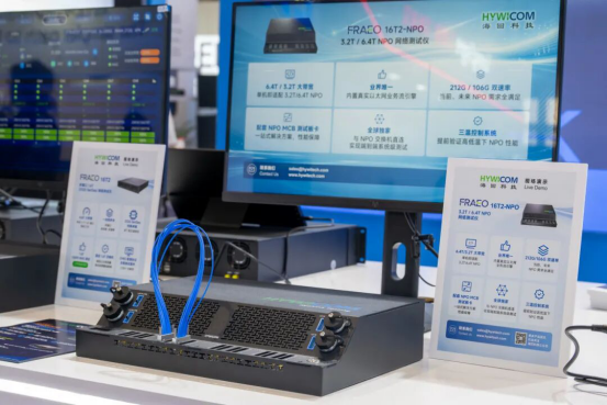
Haihui Technology launched the FRAEO 16T2-NPO network tester, supporting 32 high-speed electrical signals per unit, compatible with 106G/212G PAM4 rates, employing PRBS and L2 real business dual test engines to cover link validation through business simulation. Lianxun Instruments' 1.6T full-series test equipment has achieved mass production supply, while simultaneously developing high-speed optoelectronic hybrid ATE platforms. Wanliyan exhibited a 110GHz vector network analyzer, 1.6T network tester, and other instruments.
As optical interconnect moves toward system integration, testing work is upgrading in parallel, with evaluation focus expanding from component metrics to link integrity, business carrying capacity, and cross-component coordination performance.
Thermal Management: Liquid Cooling Accelerates Toward Scale Deployment
High-density optical interconnect brings significant power consumption increases. Air cooling's capability and space efficiency are hitting bottlenecks. Liquid cooling has transitioned from an optimization alternative to a necessary condition for scale deployment.
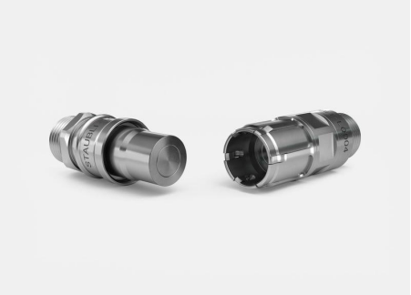
AVIC Optoelectronics' optical module liquid cooling products have already achieved volume shipments. Lingyi iTech's liquid cooling modules are expected to achieve mass production in the second half of 2026. Arade, Staubli, and Changying Precision respectively exhibited VC vapor chambers, liquid cooling quick connectors, and liquid cooling cold plates, indicating a complete liquid cooling supporting supply chain is taking shape.
Thermal management for high-density optical interconnect is not just single-module structural design, but a comprehensive engineering capability spanning optical modules, switch systems, liquid cooling piping, and data center infrastructure. Testing ensures sufficient system validation; thermal management ensures long-term equipment stability — together completing the progression from "product deliverability" to "system sustainable operation."
VII. Delivery Certainty: The Four-Layer Competitive Logic of Optical Communications 3.0
Synthesizing industry signals from IFOC and CIOE 2026, the industry's competitive logic has undergone profound changes. Single-point technology breakthroughs remain important, but the weight of large-scale manufacturing, supply chain coordination, and system integration capability has significantly increased.
First is mass production deployment. Upstream expansion is accelerating for 200G EML, InP substrates, and TGV substrates. Optical engines, external light sources, connectors, test instruments, and liquid cooling components are successively entering mass production or volume supply. Converting samples into large-volume supply requires enterprises to directly confront manufacturing realities: capacity ramp-up, yield management, supply chain assurance, and full-process customer certification.
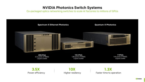
Second is system integration. High-density solutions such as NPO and CPO involve multiple links — chips, packaging, light sources, connectivity, thermal management, and testing. Single-component performance cannot determine overall solution competitiveness. NVIDIA's promotion of NVLink, Spectrum, optical interconnect, and liquid cooling system coordination essentially integrates dispersed technology links into a unified platform, converting single-point technology advantages into complete system performance. This is also the gap between leading platform enterprises and single-component manufacturers: platform enterprises can integrate full-chain resources, build complete product systems, and expand production in sync with market demand. Component manufacturers, even with leading single-point technology, still face practical obstacles in customer introduction, supply chain matching, and system adaptation.
Third is supply chain resilience.Large-scale commercialization means higher anti-risk requirements. The supply stability of core materials, optical chips, production equipment, and packaging components directly determines final delivery results. Enterprises with core link autonomous controllability, vertical integration capability, and multi-source alternative supply chains have stronger risk resistance under demand fluctuations and supply chain disruptions.
Competition in the 2026 optical communications industry is no longer simply about comparing product parameter levels. The core contest is converting technology prototypes into commercial products, scaling commercial products into volume production, integrating diverse products into complete systems, and maintaining stable delivery bottom lines under supply chain fluctuations.
Optical Communications 3.0 is not merely a speed metric upgrade, but the deep embedding of optical interconnect into computing infrastructure hardware systems.
Conclusion
The 2026 IFOC & CIOE exhibitions revealed clear industry differentiation: multiple technology routes developing in parallel, but industrialization progress among different solutions is gradually diverging. For enterprises, competitive boundaries have extended from product capability to scale manufacturing, supply chain resilience, and system integration. Technology advantages can only realize true industrial value when converted into stable capacity and sustainable delivery. Moving from "making it work" to "delivering it out" is precisely the most fundamental change in the 2026 optical communications industry.
